Here is the example block diagram for combination circuit,
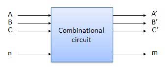
- Half Adder
- Full Adder
Half Adder
Normally, a unit which add two input variables called adder. In Half adder, it has only two inputs. It will add two single binary digits(ex- A and B). It has two outputs, SUM(s) and CARRY(c). Normally we use XOR gate for SUM and AND gate for CARRY.
Hence the main purpose of the Half Adder is, add two input bits and generate SUM and CARRY.

A
|
B
|
sum
|
carry
|
|---|---|---|---|
0
|
0
|
0 | 0 |
0
|
1
|
1
|
0 |
1
|
0
|
1 | 0 |
1
|
1
|
0 | 1 |
SUM = A XOR B
CARRY = A AND B
Here is the Block Diagram of Half Adder,
Full Adder
This kind of adders have 3 inputs. Hence it can give arithmetic sum of three input bits. The main different between of Half Adder and Full Adder is, Full Adder has "Carried In"(Cin) as well as "Carried Out"(Cout). Hence Full Adder has A, B, Cin INPUTS. A and B are the operands and Cin is a bit carried in from the previous less-significant stage.
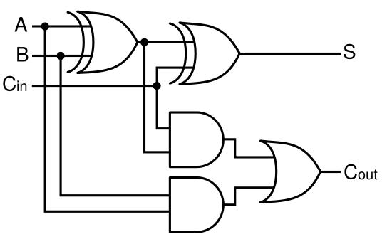

Here is the Block Diagram of FULL ADDER
